 View larger


Nand vs v nand shop
Nand vs v nand shop, 3D NAND Race Faces Huge Tech And Cost Challenges shop
$72.00
SAVE 50% OFF
$36.00
$0 today, followed by 3 monthly payments of $12.00, interest free. Read More
Nand vs v nand shop
3D NAND Race Faces Huge Tech And Cost Challenges
Figure 2 from 2D vs 3D NAND technology Reliability benchmark Semantic Scholar
232 layer NAND Micron Technology Inc
Inhibited Channel Potential of 3D NAND Flash Memory String According to Transient Time
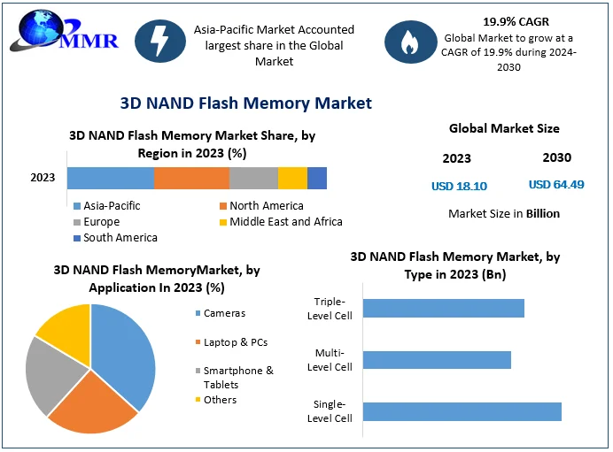
3D NAND Flash Memory Market Industry Analysis and Forecast
What is 2024 3d nand
Description
Product Item: Nand vs v nand shop
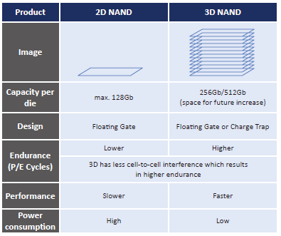
2D NAND vs 3D NAND vs V NAND How are they different shop, Vertical NAND with and without TSV a closer look shop, Difference between SLC MLC TLC and 3D NAND in USB flash drives SSDs and memory cards Kingston Technology shop, Why More Companies Are Choosing NAND Flash Memory Today The ICT Trends shop, 3D NAND How It Works Samsung SSD 850 Pro 128GB 256GB 1TB Review Enter the 3D Era shop, Samsung says 256 layer V NAND memory possible with double stack technology Yonhap News Agency shop, NAND Technology Development at SK hynix Reaching New Heights SK hynix Newsroom shop, Samsung s V NAND Hitting the Reset Button on NAND Scaling shop, Comparison of 3D NAND structures between BiCS Toshiba and VSAT Our. Download Scientific Diagram shop, Samsung 850 EVO SSD With 3rd Gen 48 Layer V NAND Performance Comparison The SSD Review shop, What Is 3D NAND Types Pros Cons ESF shop, Intel promises 10TB SSDs thanks to 3D Vertical NAND flash memory KitGuru shop, Flashback The Evolution of NAND Flash Technology SK hynix Newsroom shop, What is 3D NAND flash Definition from TechTarget shop, 41KB 2001 null null null 3 null null 3 1 2003 null I4 DzaDdUaNQPM shop, News Understand the difference between different grades of SSD Chips of NAND Flash SLC MLC TLC QLC shop, 2D NAND vs. 3D NAND Pure Storage Blog shop, NVMe vs. NAND Technologies Understanding the Basics NVM Express shop, Samsung V NAND A Landmark of the Hyperscale AI Era Samsung Semiconductor EMEA shop, 3D NAND vs 2D NAND Challenges in Industrial Applications shop, How 3D NAND Can Continue Gigabytes Scaling Enhance Applications SD Association shop, 3D NAND Flash Wars Begin shop, 3D NAND vs 2D NAND What s the Difference in NAND Flash Memory shop, Schematic diagrams of 3D NAND architecture a vertical gate and b Download Scientific Diagram shop, 96 layer 3D NAND Flash Transcend Information Inc shop, 3D NAND Flash memory Making HDDs obsolete in a data centric economy shop, 3D NAND Structure 3D Metrology Illuminating Semiconductors shop, 3D NAND Race Faces Huge Tech And Cost Challenges shop, Figure 2 from 2D vs 3D NAND technology Reliability benchmark Semantic Scholar shop, 232 layer NAND Micron Technology Inc shop, Inhibited Channel Potential of 3D NAND Flash Memory String According to Transient Time shop, 3D NAND Flash Memory Market Industry Analysis and Forecast shop, What is 2024 3d nand shop, 2D NAND vs 3D NAND vs V NAND How are they different shop, Tech Brief Memory Grows Up with 3D NAND shop.
2D NAND vs 3D NAND vs V NAND How are they different shop, Vertical NAND with and without TSV a closer look shop, Difference between SLC MLC TLC and 3D NAND in USB flash drives SSDs and memory cards Kingston Technology shop, Why More Companies Are Choosing NAND Flash Memory Today The ICT Trends shop, 3D NAND How It Works Samsung SSD 850 Pro 128GB 256GB 1TB Review Enter the 3D Era shop, Samsung says 256 layer V NAND memory possible with double stack technology Yonhap News Agency shop, NAND Technology Development at SK hynix Reaching New Heights SK hynix Newsroom shop, Samsung s V NAND Hitting the Reset Button on NAND Scaling shop, Comparison of 3D NAND structures between BiCS Toshiba and VSAT Our. Download Scientific Diagram shop, Samsung 850 EVO SSD With 3rd Gen 48 Layer V NAND Performance Comparison The SSD Review shop, What Is 3D NAND Types Pros Cons ESF shop, Intel promises 10TB SSDs thanks to 3D Vertical NAND flash memory KitGuru shop, Flashback The Evolution of NAND Flash Technology SK hynix Newsroom shop, What is 3D NAND flash Definition from TechTarget shop, 41KB 2001 null null null 3 null null 3 1 2003 null I4 DzaDdUaNQPM shop, News Understand the difference between different grades of SSD Chips of NAND Flash SLC MLC TLC QLC shop, 2D NAND vs. 3D NAND Pure Storage Blog shop, NVMe vs. NAND Technologies Understanding the Basics NVM Express shop, Samsung V NAND A Landmark of the Hyperscale AI Era Samsung Semiconductor EMEA shop, 3D NAND vs 2D NAND Challenges in Industrial Applications shop, How 3D NAND Can Continue Gigabytes Scaling Enhance Applications SD Association shop, 3D NAND Flash Wars Begin shop, 3D NAND vs 2D NAND What s the Difference in NAND Flash Memory shop, Schematic diagrams of 3D NAND architecture a vertical gate and b Download Scientific Diagram shop, 96 layer 3D NAND Flash Transcend Information Inc shop, 3D NAND Flash memory Making HDDs obsolete in a data centric economy shop, 3D NAND Structure 3D Metrology Illuminating Semiconductors shop, 3D NAND Race Faces Huge Tech And Cost Challenges shop, Figure 2 from 2D vs 3D NAND technology Reliability benchmark Semantic Scholar shop, 232 layer NAND Micron Technology Inc shop, Inhibited Channel Potential of 3D NAND Flash Memory String According to Transient Time shop, 3D NAND Flash Memory Market Industry Analysis and Forecast shop, What is 2024 3d nand shop, 2D NAND vs 3D NAND vs V NAND How are they different shop, Tech Brief Memory Grows Up with 3D NAND shop.